Update 2023-02-18: There's a new version of this design: v2.1
I don't consider this design done; but, I've gotta start writing it down because I'm carrying too much diagnostic info in my head regarding this thing.
One of the early kit's I built was this AI011 VCO. Despite the website saying it uses a Curtis chip (CEM3340) mine came with a clone AS3340A. At the time I didn't know anything about either chip, I just wanted a VCO to build and play with. Overall it is a fine VCO, it sticks to the datasheet's circuit for trimming. I also built four Befaco Even VCOs to use with the polyphonic envelop generator. I was initially on the fence about building my own, but I eventually decided it would be a nice accomplishment to do an entire signal chain from keyboard to output all of my own designs and an oscillator was gonna be necessary.
So I bought some AS3340's from Electric Druid and set about making my own design.
The AS3340 has a triangle, falling sawtooth and pulse output. It has frequency, pulse width, sync inputs. It seems common to add a sine wave generator output with external circuitry, but I felt that would overcomplicate this first design (it also seems like an interesting thing to have as a separate module).
The data sheet for this is severely abridged as are most of the Alfa chips data sheets. They lean heavily on the original Curtis (CEM) chip data sheets. It's basically impossible to design something with only the Alfa data sheets. This is by far my main criticism of these chips. They work fine, but the documentation sucks. You'll need to find the CEM3340 datasheet for this, but not the 2 page one, you need the full version which offers 6 pages of glorious information. Here's where I found it.
I started this design on the breadboard, as usual.

It's on the left side of that breadboard the center and right side are some LFO designs. I recently bought more breadboards to deal with this congestion, but this is from before they showed up. I knew much of the testing I'd need to do wouldn't matter if I did it on the breadboard. I wanted to make a mostly surface mount design and that meant I just had to get a PCB made and play with that instead.
I did make a few simulations of the output stage(s): https://tinyurl.com/2ew2cxa8
The biggest difference between my circuit and the datasheet is that I've opted for the 'easier' trimming described in 'Tuning the AS3340' by Rob Hordijk. Also available here. That circuit should result in a single pass tuning, unlike the other VCOs mentioned above that require multiple passes. In that respect it works, if the circuit is correct and other variables controlled, but that proves difficult as we'll see.
So I went forward with the idea and got some v1 PCBs. When I received them I assembled one and started test and immediately found several issues. But before I get into that, here's what it looks like:


Testing and Issues
Anyways lets dig into the issues the v1 board has.
Lets start with the easy stuff.
- When making the front panel drawings I noticed the fine tune pot and PWM pot are not equally spaced from the center line. Also the jacks centers are not equidistant from the sides making front panel layout awkward. I made the whole PCB off center relative to the front panel to mitigate this.
- I removed R6. R6 was meant to be a pulldown for the buffer input that I've used in other designs but here it interfered with the R7/R8 voltage divider causing lower than expected output.
- JP1 isn't necessary. I think I added it to help isolate the frequency inputs for testing, but I haven't really used it and I've shorted it on all the PCBs so far.
- I've changed R10 to 47k (from 50k). I thought I'd need two resistors to get 51k, turns out that's a more standard value than 50k. So now R10 is a 47k and R9 is shorted. I don't know if 51k or 47k is better. I see designs with both. There are other 47k's on the PCB so in an effort to reduce component variety I think 47k is ok.
- R21 & R23 are 5.1k. Again I didn't look up common sizes on that so 5.1k is just a nearest value I had on hand. I still haven't tested the HF tracking so who knows if they are okay.
- RZ1 is 18k not 13k. I don't remember exactly why, but I think it was because 13k wouldn't let me fully trim out the voltage difference between TP1 and TP2 as required by the trimming process.
- JP3 10uF polarized cap from -5 to -12 rail.
- JP2 short - by design for the -5V supply.
- R5 short - hack that ties one side of JP3 to -12V to allows JP3 to be used for the 10uF cap.


When I had removed those there was another issue, my 12V rail was at 11.25V. As it turns out I didn't verify that or didn't think it would matter but this circuit is super sensitive to input voltage and CV voltages. That was a face palm moment. I dug up the data sheet for the Mean Well RT65B and I can see that the 11.25V is in spec (barely) but they also have a diagram and a note that 10% load on the 5V rail is needed. Forums also confirm that the supply needs a load on the 5V rail. The trim pot for the 5V rail effects the other rails. I've ordered some load resistors to put on the supplies but for the time being just trimmed them higher so that I get a proper 12V rail.
With all of that fixed the oscillators worked a bit better. They're still a little bit off in the 1V tracking but I think that's still a minor voltage difference between the bench and the rack supplies. I need to get both more consistent to really sort this out. That said v2 will place the trim pots on the other side of the PCB so I can calibrate them in situ.
2022-08-28 - Testing Notes:
Did a bunch of testing with a frequency counter.
Completely recalibrated all four DUTs with frequency counter and mV scale for temp adjust step 1.
The tracking from 0v to 5V looked pretty good using a bench supply for CV and multimeter with mV accuracy. Frequency counter struggled a bit at some frequencies, so I compared it against an oscilloscope at lower frequencies.
Procedure was:
- Powered on for 1hr or more to warm up.
- Readjusted temp1 w/ mV range on multimeter, drifts a bit, got it under a mV.
- Short J4 and get 1046.5 with ref pitch trim pot.
- Set Fine Tune knob to center.
- Set Freq knob to 0, full CCW.
- Input CV 5.000V±0.001
- Use Re-find C6 trim pot to get 1046.5, this was trickier than with F4 shorted.
- Input CV 0.000V±0.001
- Use scale adjust trim pot to get 32.70±0.01 Hz
- Check tracking.
| CV | DUT1 | DUT2 | DUT3 | DUT4 | Ideal (Hz) |
|---|---|---|---|---|---|
| 0V | 32.7 | 32.7 | 32.7 | 32.7 | 32.7 |
| 1V | 65.45 | 64.9 | 66.0 | 66.0 | 65.41 |
| 2V | 130.9 | 130.2 | 130.7 | 130.6 | 130.81 |
| 3V | 261.9 | 260.8 | 261.8 | 261.4 | 261.63 |
| 4V | 523.3 | 521.6 | 523.4 | 522.5 | 523.25 |
| 5V | 1047 | 1045 | 1049 | 1046 | 1046.5 |
I think I'm okay with that tracking. It's usable if the power supply is okay.
2022-09-04 - Testing Notes
Today I decided to test the warmup time on the circuit. I measured the AI011 and my circuit. Here's the results:
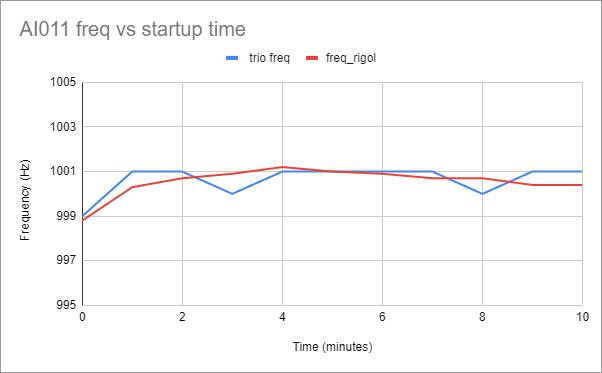
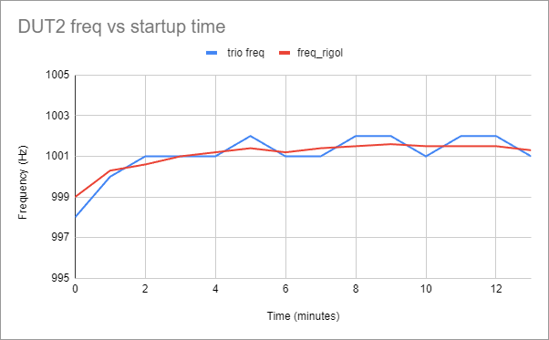
- Room temperature devices (off overnight).
- 5V CV input and I briefly (20 seconds or so) turned them on to get them close to 1000Hz with the knobs
- Turned them off a few minutes.
- Turned on and recorded data for 10+ minutes.
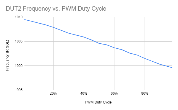
- Double check output voltages and adjust gain resistors.
- Buy and try higher precision resistors R30, R2
- Most design and the data sheet show higher precision resistors that I used, they're hard to find though.
- I haven't messed with high freq. track adjustment at all yet.
- Fine tune knob has a little too much influence on tune, several semi tones... reduce?
- Increase R3 or reduce range of RFINE_TUNE1
- Try 5.6k on R21,R23 to reduce component count.
- I've got three different caps for CF1/CF2 on different PCBs.
- I need to choose one type but I'm not sure how to decide yet.
- This list isn't complete, I need to use the v1 more and get through the rest of the testing.
- Add precision resistor footprints. I can't buy them but might as well prepare for if I find them.
- Fix -5V regulator output capacitance.
- Add 100pF cap in parallel with R10.
- Remove JP1
- Remove R6
- Remove R9
- Remove alternate supply (-12V paths for VEE)
- Add a resistor for the 'hysteresis' mentioned in forums.
- Fix resistor values from experimentation.

This work is licensed under a Creative Commons Attribution-NonCommercial-ShareAlike 4.0 International License.
Comments
Post a Comment
Comments are moderated. Comments containing links are marked as spam.