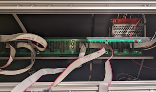
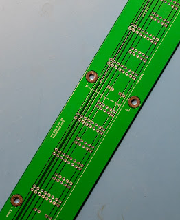
For the Eurorack cabinet I built, I needed a way to distribute power to all the modules. My old had Behringer power supplies with 'flying bus' cables (flat cables with female connectors). In the cabinet I wanted something more robust/fixed to the cabinet so I designed my own PCB. It has very little actual circuitry on it, it's mostly just traces and connectors with a few caps here and there. No rigorous design went into this, I just looked about on the web for similar solutions and them made my choices based on components I had.
Assembly Order
- Resistors
- LEDs
- 2x5 and 2x8 sockets, only 1 or 2 pins on CV/Gate lines (which have lower heat sink capacity)
- Caps on +/- 12 Rails (skip the ground pin)
- Finish soldering all pins with extra hot air preheating the board. This was absolutely necessary on the 2oz copper because the heat sinking capacity of this PCB is huge.
The v1 schematic didn't have a value for the LED's resistors. 1kΩ works just fine.
As usual this design is available here if you would like to have some fabricated for your use. I specified 2oz copper instead of the usual 1oz on most PCBs and that cost a bit more (probably wasn't necessary either). Because of the size they aren't super inexpensive they were a bit over $5 each, still way less than buying them premade.
I assembled another one to have at my workbench and printed a few brackets to hold it in place.
Design files: https://github.com/EchelonForce/eurorack_power_strip
This work is licensed under a Creative Commons Attribution-NonCommercial-ShareAlike 4.0 International License.


(Hi - looking at your design in KiCad, I was wondering why you added the second GND layer, which eradicated all of the thermal relief on the pads. Unfortunately, I didn't check until I had 5 boards made, which are virtually omposdible ti solder. Why wreck a goid design?
ReplyDeleteThese are definitely complicated to solder. I've assembled 16 or so of the original batch. What I've found that works is to set up a hot air on some helping hands so that it's aimed a few centimeters ahead of where your soldering and let it preheat the board. I hold all the components in with a long strip of foam so I don't have to do anything but chase the hot air around with the soldering iron. As for why the thermal relief was removed, this was an early design and I don't think I had figured out yet how to manipulate all the settings in kicads filled regions. So at the time letting the default settings add thermal relief resulted in very thin traces for the ground and power rails at each connector. I wanted the traces to be as wide as possible so that I didn't have to worry about the current carrying capacity while daisy chaining these. Now that I've actually built with them and used them, the traces probably don't need as much capacity as I gave them.
ReplyDeleteThat explains a lot - thanks for making the design open source, I got 5 boards from JLCPCB for £31, and am getting better at soldering them. Hot air is definitely needed in addition to the soldering iron. I've got my hot air gun held in a flexible phone mount!
Delete