This post is about a DIY design of a polyphonic envelope eurorack module.
The idea for this module started after I bought a second hand Roland System-8 and started to understand the polyphonic features better. I had already built several oscilators from a few DIY kit providers and was running into the issue of not having enough envelopes for them all. So decided to try and build a polyphonic envelope.I jumped right into this design with a chip selection, I went over to Electric Druid and grabbed a few AS3310 ADSR chips to experiment with. I didn't have any modules that used this chip but while breadboarding a design I came across a useful reference on Eddy Bergman's site. Ultimately my goals of a polyphonic version complicated the design a bit.


Assembly order is unique to every PCB depending on the BOM, here's the order I assembled in:
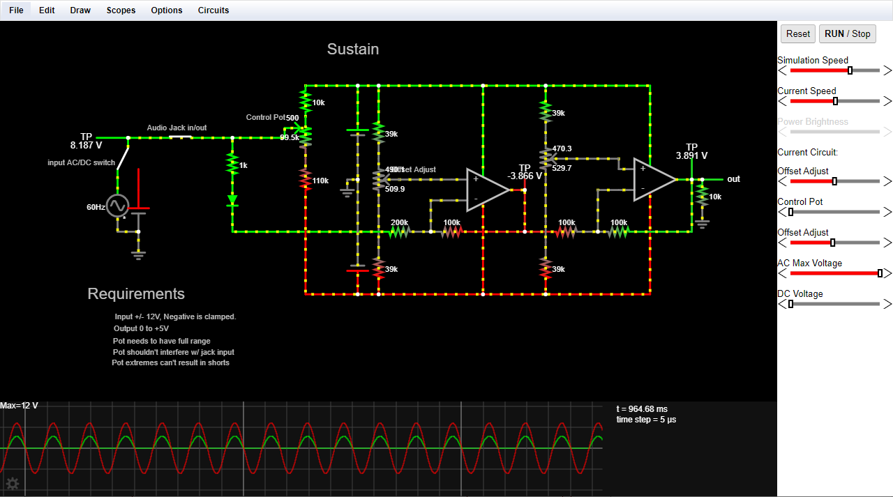
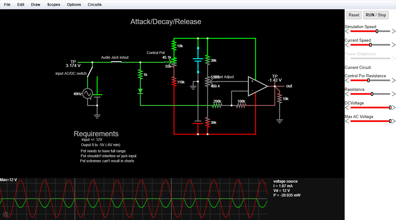
One thing to note on the AS3310 is that is has some odd control voltages, particularly the Attack, Decay and Release CVs are 0 to -5V instead of 0 to +5V like the Sustain CV. I wanted 0 to 10V tolerant CV inputs and potentiometers too. To solve that oddity I decided to simulate the CV input buffering I'd need to work with the chips.
Sustain CV Simulation: see it live
Attack, Decay, Release CV simulation: see it live
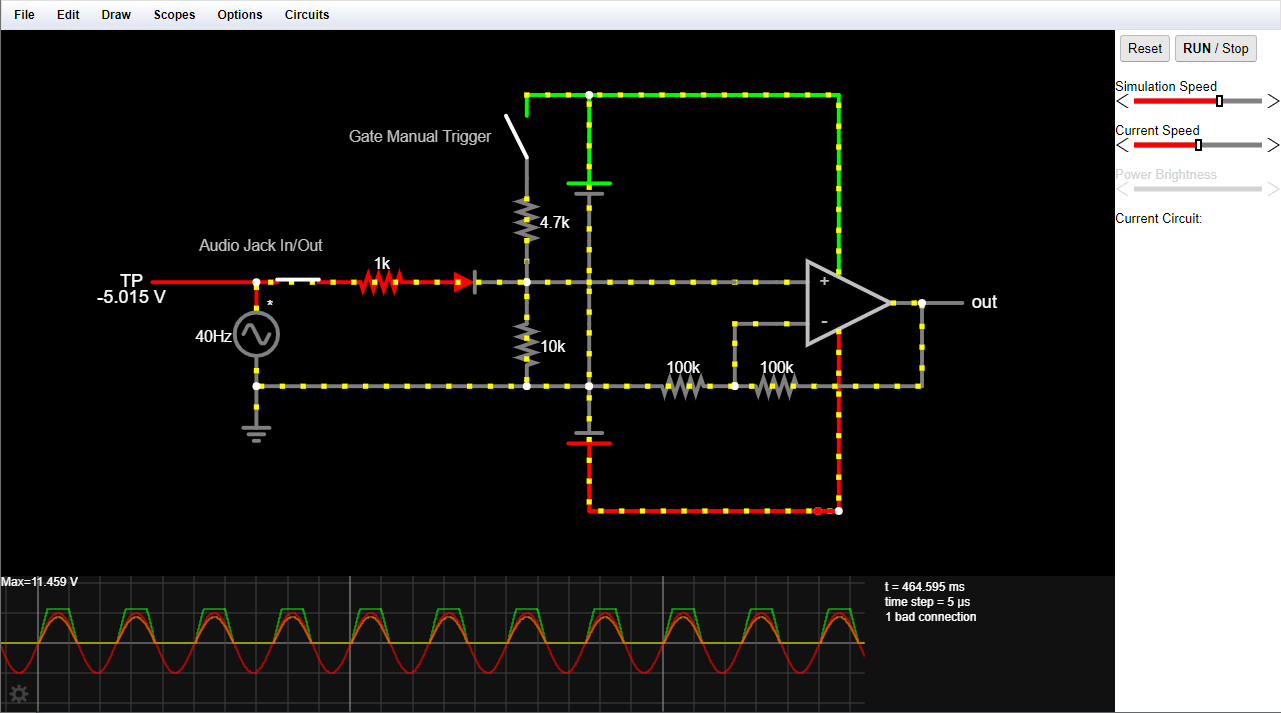
For the Gate inputs I also wanted 10V tolerance, so I used an op-amp there to buffer and amplify it before the chip sees it.
Gate simulation: see it live
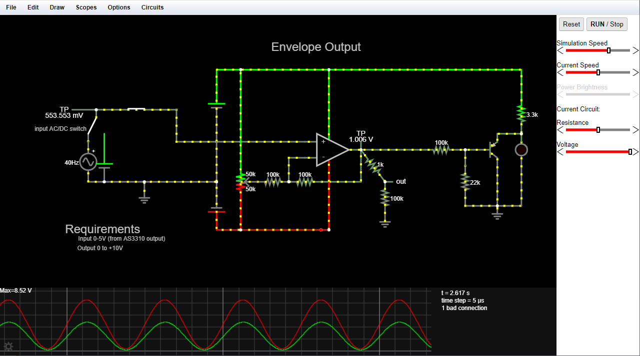
On the output side I wanted to amplify the AS3310's 0 to 5V outputs to 0 to 10V and also wanted to have a buffer between the output jack and the chip.
Output Buffer Simulation: see it live
With some simulations functional I went about breadboarding the design to see if it would work as expected. For the breadboard version I only used one AS3310, so it's not polyphonic yet, I just wanted to prove the ideas and circuits before adding more complexity.

That worked out pretty well. I can safely say it's the most complicated thing I've put on a breadboard since college.

After that I designed a version with 4 AS3310's to make the first version of the polyphonic envelope module in KiCAD. One thing I discovered during this was that the hierarchical sheets are a useful way to organize parts when they're added to the PCB. If every part of the schematic was on one page, then all the parts for the design get jumbled together on the PCB, but the parts in a hierarchical sheet are separate from the rest. So in the schematic files there are several sheets to take advantage of this quirk and also it makes block diagrams of the overall design as a side effect.
On the PCB I also added a switch to bypass the gate and trigger all the envelopes for testing. Unfortunately I didn't simulate that idea, or breadboard it, so it was wrong. On the versions I've built so far I just leave a few components out and only the first envelope uses the switch. More on that later.
The PCB was complicated. I was set on a two layer PCB and very quickly I switched the resistors on the BOM to be surface mount instead of through hole. I think I routed the PCB two or three times from scratch before I ordered them.
I ordered the v1 PCBs for this on January 13th. I didn't receive them until late in April. I used the service Seeed Fusion which has very inexpensive boards, but I learned from this order that you should always choose the fast shipping option(s). They simply sat on this design for almost 4 months before it moved through production. I reached out to them several times and got excuses for holidays and lockdowns, but I also ordered other designs after these and received them before these, so I have a hard time trusting those excuses.


- Resistors - all surface mount components, both sides of the PCB.
- Diodes and Ferrites
- Small Caps
- Sockets
- Large Caps
- Transistors
- Trim Pots
- Jacks, LED and Pots in panel


Problems on v1 PCB:
- Output LEDs always were always on.
- Reversed transistors. See orientation in sim.
- Fix: rotate Q1,Q2,Q3,Q4 180 (swap collector/emitter in schematic)
- Only first envelope working. - didn't solder U7 properly...
- Switch triggers first envelope.
- Every gate input triggers every envelope. On v1 going to have to remove 4.7k's that connect to switch.
- Here's a simulation of it misbehaving.
- Remove: R4, R6, and R16
So far I've built two of the envelopes and tested/used them in my synth.


2022-08-16 Testing:
On the third v1 build of this I discovered that the attack and decay times weren't respected when a gate signal was used. On the scope it looked a lot like the 'Q1 Disabled ***' note in the datasheet. So I started to probe around for that issue. I also checked the gate button, but it seems to work most of the time.
Eventually I discovered the trigger pin on the chip wasn't really changing when an LFO or similar signal was passed in. It seems those signals didn't have sharp enough edges to cause the trigger spike needed.
I played around with the simulation a bit an found that a larger value decoupling cap on the trigger improves the trigger signal timing. On hardware a 1uF (instead of 3nF) seems to work. It's probably too big but it's available and functions. Some simulation.
Here's a scope image showing the trigger (channel 2) missing on the rising edge of the gate (channel 1).


Changes for v2:
- Fix transistor orientation.
- Move R15 label it's confusing.
- Make all U# labels visible, not hidden by chips/sockets.
- Remove R4, R6 and R16 or fix gate switch circuit.
- Need to figure out a way for switch to trigger but not allow other gates to go high. Maybe tie it to trig input on AS3310 and remove ugly 3nF?
- Label Pots on silkscreen
- Some CV pots might not be needed? Investigate.
- 3nF caps might not be needed. Need to evaluate v1 PCB with other values.
- Use geographic re-annotate to make the resistor values easier to find during assembly.
Design files and CAD:

Comments
Post a Comment
Comments are moderated. Comments containing links are marked as spam.