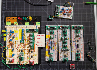
One of the first things I bought when I started messing with my own synth designs was a few of these red break out boards for audio jacks.
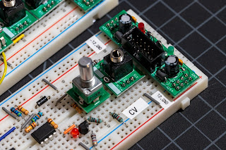
So I came up with my own designs for a few break out boards for common stuff.
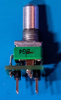
There's a BOB for the alpha pots I've been using. It's also possible to put the ubiquitous 4 pin momentary push buttons on this PCB, but that's a hack...
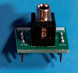
Another for the MJ-355W jacks I've been using but it also fits Thonkiconn jacks.
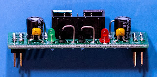
And one more for the typical power supply I've been putting in modules.
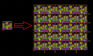
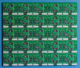
There's really nothing too special about these but it was a good exercise to go through to figure out how Seeed's PCB panelization works.
As it turns out panelizing the designs is a pretty easy step, I've just been doing it manually and the results have been good. In general the steps (in KiCad) are:
- Make sure you're done with the design and the DRC works as expected, any changes after panelization is done either needs to be done N times all over the panel or you have to re-panelize.
- Save the finished original PCB as a new file e.g. jack_bob_panelized.kicad_pcb (kicad may generate some other files, but I just ignore them.
- Select the entire board and copy pasted it to fit just inside the fab house's PCB limit (100x100mm) in the case of Seeed
- The Special Tools>Create Array tool can do this too, but it might reannotate the parts which isn't desirable, check the 'Keep existing reference designators box' to prevent that)
- Line up the original board's Edge.Cut layer (the board outlines). It helps to use snapping to the grid for this.
- Remove extraneous Edge.Cut geometry. The pasted board outlines have a lot of overlapping lines, I draw new extra long lines over those and then remove the old ones, leaving only the minimum set of lines on the layer, so that it's clear where the milling should happen. (this is required according to their spec. "The v-cut line must go across the entire length of the boards".
- Add the required 'V-CUT' text on the Edge.Cut layer. I also orient these to the line they are near.
- Save the ...panelized.kicad_pcb.
- Generate outputs for the pcb layers and order.
It's looks like a lot in text, but in practice it's a pretty simple set of steps to do right before ordering. If I find some issue on the design I just redo the steps after fixing the original. I treat the panelized design as a generated output and don't really archive it.
As for assembly, these are really simple, my recommendation on stuff like this would be to make several at once and leave the PCBs connected so that you don't have tiny PCBs to handle.
Issues in these BOB designs:
The pot design is a bit easy to assemble wrong, if the potentiometer is populated first then it's impossible to screw up but hard to solder. I don't think this is worth fixing because it's a tradeoff to get the PCBs to be small enough to optimize the breadboarding a bit better.
The power supply PCB works fine and is good for me because it represents the modules actual power supply circuitry with a minimal breadboard foot print. The ferrite beads are probably completely unnecessary for most designs, I have a few digital things in some designs that might need one. Mostly I was copying other kit's circuits, but there's little evidence that they're necessary. One thing I'd change if I ordered more would be to switch the -12 and GND rails where the plug into the breadboard. It seems there reversed from how my bread board's rails are labeled which is a good way to get -12V into a ground or 24 volts across something. The resistors for the LEDs would be easier to alter if they were on the other side of the board. When I panelized this it was under the minimum width allowed by Seeed, so they had to add some extra are outside my design to hold it. That was my first experience with them reporting an issue on an order. They're site is pretty well set up for that though so it was quick to communicate the fix I preferred.
As it is, by panelizing these designs and getting the minimum count of 10 from Seeed, I've basically got a lifetime supply for way less than I'd have paid to get them elsewhere.
These designs are available here:
https://github.com/EchelonForce/alpha_pot_bob
https://github.com/EchelonForce/audio_jack_bob_MJ-355W
https://github.com/EchelonForce/eurorack_to_breadboard_psu
This work is licensed under a Creative Commons Attribution-NonCommercial-ShareAlike 4.0 International License.


Comments
Post a Comment
Comments are moderated. Comments containing links are marked as spam.